

Institute of Applied Physics, Abbe Center of Photonics, Friedrich-Schiller-Universität, Jena, Germany
Fraunhofer-Institute for Applied Optics and Precision Engineering IOF, Jena, Germany
Max Planck School of Photonics, Germany
Integration of two-dimensional materials in optical systems for nonlinear optics, sensing, and single photon sources
Many of crystalline two-dimensional materials have been discovered in the last years, a lot of which exhibit interesting physical properties. They are a natural addition to the set of common of optical materials and can be used to functionalize classic micro- and nanooptical systems. Moreover, they grow in a crystalline manner on many substrates commonly used in photonics, such as SiO2, Si, and Al2O3. From an optics point-of-view transition-metal dichalcogenides [1] (TMCs) and hexagonal Boron-Nitride [2] (hBN) are among the most interesting materials. TMCs are direct semiconductors with bandgaps in the visible. They exhibit unusually high refractive indices, strong and highly sensitive fluorescence [3], and large nonlinear coefficients [4]. Their light-matter-interaction behaviour is dominated by highly stable excitons and valley-polarization [5]. hBN, on the other hand, is a large bandgap dielectric, which exhibits bright room-temperature defect-state single-photon emitters [6, 7].
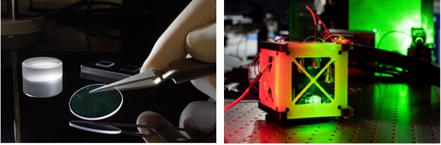
I will discuss some strategies to integrate 2D-materials with coatings, resonators, and waveguides. We use an IAPVD-based low-temperature technique to embed 2D-materials in planar dielectric systems [8], such as optical coatings and Bragg-cavities, without degradation of their properties. There we have studied the strong coupling of excitons to cavity polaritons and their coupling to external magnetic fields [8] as well as the resonator-based enhancement of single-photon-emitters [7]. We also show, that they can be integrated in optical systems [9] for usage in space-based quantum key distribution networks [10]. I will also discuss experiments, where the material is coupled to all-dielectric nanoscale resonators [11]; paving the way for active nanoscale photonic structures. Another topic is the integration of 2D-materials with optical fibers and nanophotonic waveguides. These waveguides enhance light-matter interaction radically and enable sensing applications and applications in low-power nonlinear optics.
References
[1] K. F. Mak, C. Lee, J. Hone, J. Shan, and T. F. Heinz, Atomically Thin mos2: A New Direct-Gap Semiconductor, Phys. Rev. Lett. 105, 136805 (2010).
[2] L. Song, L. Ci, H. Lu, P. B. Sorokin, C. Jin, J. Ni, A. G. Kvashnin, D. G. Kvashnin, J. Lou, B. I. Yakobson, and P. M. Ajayan, Large scale growth and characterization of atomic hexagonal boron nitride layers, Nano Letters 10, 3209–3215 (2010). PMID: 20698639.
[3] A. Splendiani, L. Sun, Y. Zhang, T. Li, J. Kim, C.-Y. Chim, G. Galli, and F. Wang, Emerging Photoluminescence in Monolayer MoS2, Nano Lett. 10, 1271–1275 (2010). PMID: 20229981.
[4] N. Kumar, S. Najmaei, Q. Cui, F. Ceballos, P. M. Ajayan, J. Lou, and H. Zhao, Second harmonic microscopy of monolayer MoS2, Phys. Rev. B 87, 161403 (2013).
[5] K. F. Mak, K. He, J. Shan, and T. F. Heinz, Control of valley polarization in monolayer mos 2 by optical helicity, Nature nanotechnology 7, 494 (2012).
[6] G. Grosso, H. Moon, B. Lienhard, S. Ali, D. K. Efetov, M. M. Furchi, P. Jarillo-Herrero, M. J. Ford, I. Aharonovich, and D. Englund, Tunable and high-purity room temperature single-photon emission from atomic defects in hexagonal boron nitride, Nature communications 8, 705 (2017).
[7] T. Vogl, Y. Lu, and P. K. Lam, Room temperature single photon source using fiber-integrated hexagonal boron nitride, Journal of Physics D: Applied Physics 50, 295101 (2017).
[8] H. Knopf, N. Lundt, T. Bucher, S. Höfling, S. Tongay, T. Taniguchi, K. Watanabe, I. Staude, U. Schulz, C. Schneider, and F. Eilenberger, Integration of atomically thin layers of transition metal dichalcogenides into high-q, monolithic bragg-cavities: an experimental platform for the enhancement of the optical interaction in 2d-materials, Opt. Mater. Express 9, 598–610 (2019).
[9] T. Vogl, R. Lecamwasam, B. C. Buchler, Y. Lu, and P. K. Lam, Compact cavity-enhanced single-photon generation with hexagonal boron nitride, ACS Photonics in publication (2019).
[10] T. Vogl, K. Sripathy, A. Sharma, P. Reddy, J. Sullivan, J. R. Machacek, L. Zhang, F. Karouta, B. C. Buchler, M. W. Doherty et al., Radiation tolerance of two-dimensional material-based devices for space applications, Nature communications 10, 1202 (2019).